 |
Step height
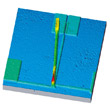
Metrology 3D Step Height Provides the height difference between two planes defined by two areas on a surface. The first area is defined as the reference and the software fits a least squares plane through this area. The second plane is then measured from this. As well as mean step height, maximum height and minimum height, the angle difference is also measured.
2D Step Height
ISO 5436-1 Step Height |
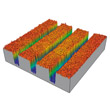
MEMS & nanotechnology
Metrology Roughness Accurate measurement of roughness within MEMS devices allows surface interactions to be controlled, whether they are solid to solid interactions as in micro gear systems or solid to liquid as found in micro fluid pumps.
Step Height
Lateral Dimensions |
Laser etch measurement
Metrology Step Height As IC packages have become smaller and thinner the requirement for measuring step height of laser etching has become more important. The target depth of the laser etch is defined by two requirements. Firstly, it must be deep enough to provide tamper proof marking that can be read by IC identification systems and secondly, it must be shallow enough not to damage the circuits on the chip.
Roughness |
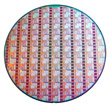
Epitaxial wafers
Metrology Surface Roughness Surface texture is a vitally important parameter in specifying the quality of epitaxial semiconductors for both customers and suppliers. With the current drive for ever smaller circuits to be printed on wafers, the tolerances for roughness are becoming tighter. Surface finish for epiwafers is specified in nm, this requires a system with very low noise and high resolution be used to measure them. |
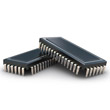
IC package measurement
Metrology Flatness Matching the flatness of the die with that of the die seating area is important to reduce stress placed on the IC during the packaging process and throughout the operation of the device. Controlling the flatness of the overall package is also necessary to ensure correct placement of the IC and good electrical contact being made when soldered.
Roughness
Step Height |
 More Information