 |
| |
|
|
|
| |
|
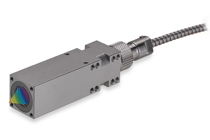
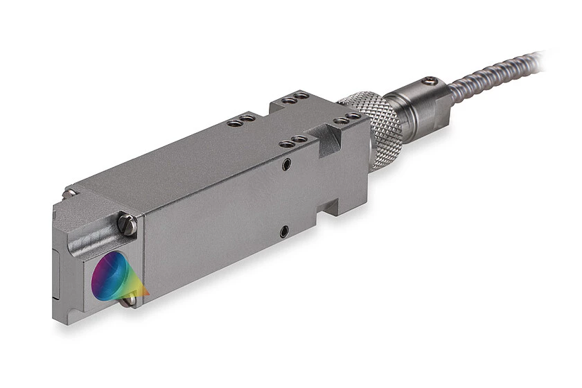
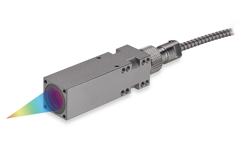
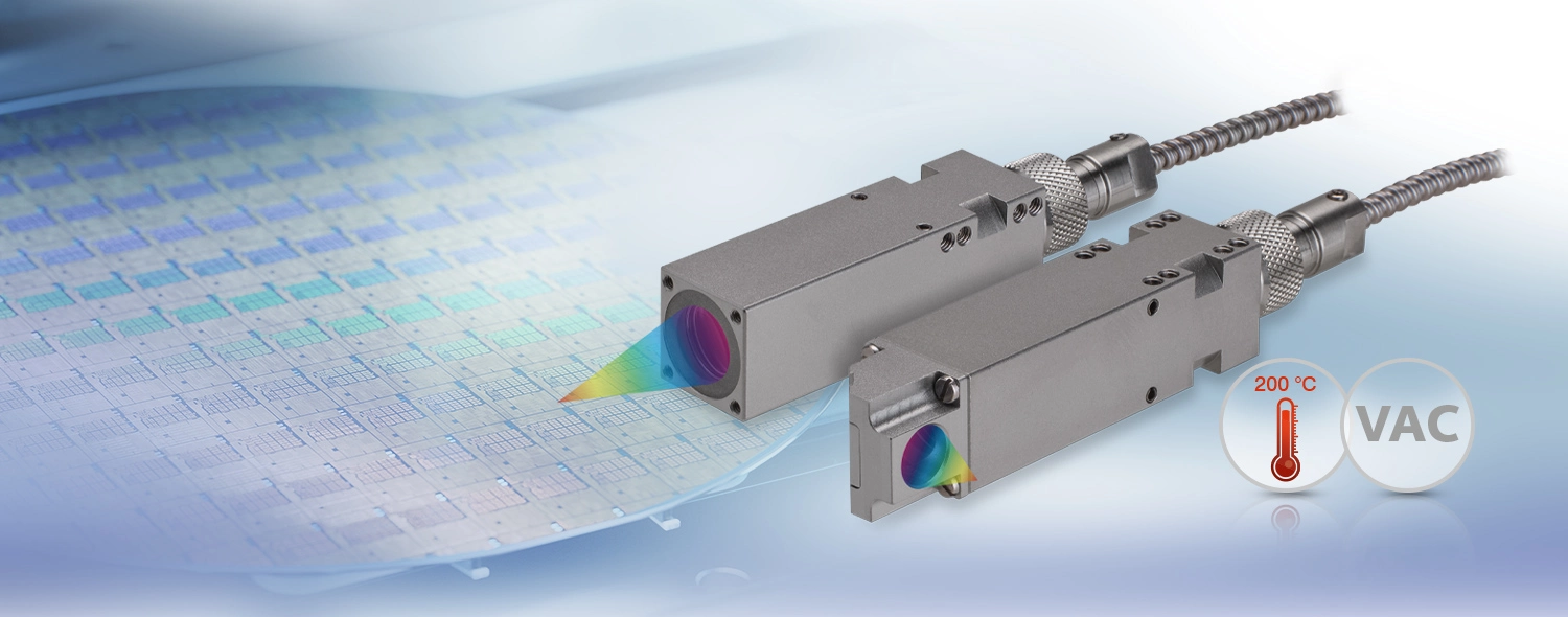
Confocal high temperature sensors for environments up to 200° C
|
| |
| The new confocal chromatic high-temperature sensors set standards for measurements in demanding environments. For the first time, the Micro-Epsilon portfolio includes optical sensors that can withstand temperatures up to 200 °C - with maximum measurement accuracy. Thanks to their compact design, these sensors are ideal for applications with very limited installation space. The innovative HT models are available in various measuring ranges and with a 90° beam path, and can be flexibly adapted to different installation situations. Due to minimal outgassing, the sensors are suitable for use up to ultra-high vacuum (UHV) - perfect for measurement tasks in precision machine building and the semiconductor industry. |
| |
|
confocalDT IFS2407-0,8HT/VAC
|
| |
|
|
| |
|
confocalDT IFS2407-2HT/VAC
|
| |
|
|
| |
|
confocalDT IFS2407-4HT/VAC
|
| |
|
|
| |
| |
 |
| |
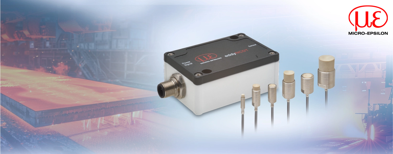
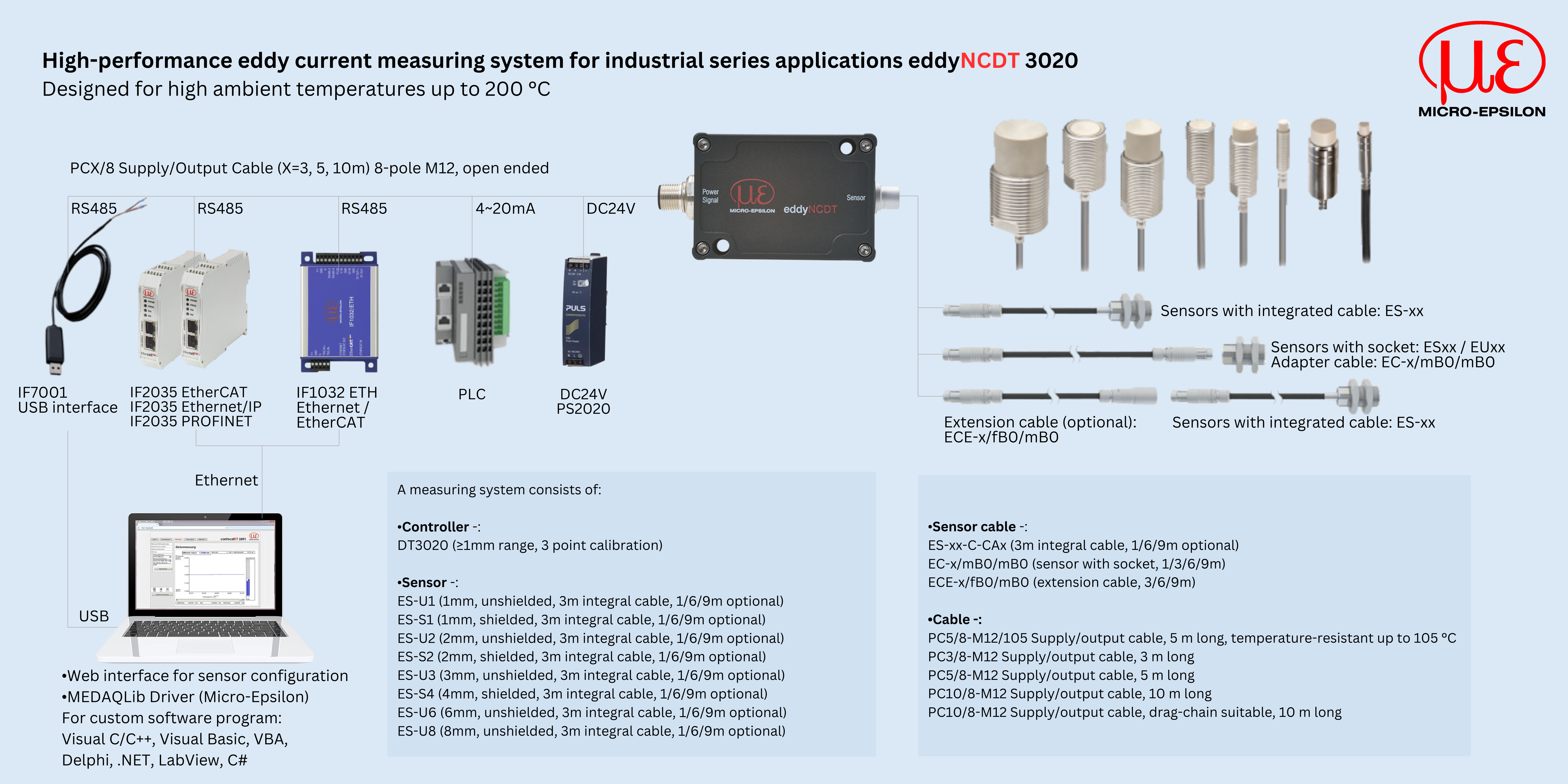
High-performance eddy current measuring system for industrial series applications  Product Technology Product Technology
|
| |
|
|
| |
 |
|
|
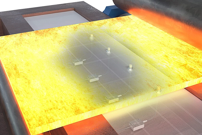
The eddyNCDT 3020 is a compact and powerful inductive measuring system (eddy current) for fast and precise displacement, distance and position measurements in industrial applications. Flexible in terms of connectivity and easy to configure, it can be used for numerous measurement tasks in industry and machine building.
|
| |
|
The sensor system is designed for series and OEM applications and delivers precise and stable measurement results even under harsh conditions - up to max. 200 °C ambient temperature. The robust controller can be combined with a wide variety of sensors and is factory-adapted to ferromagnetic or non-ferromagnetic materials.
|
| |
| Robust and precise - for industrial series applications at high temperatures. |
| |
|
|
|
|
|
Extremely high temperature application range of the controller up to 105 °C
The robust DT3020 can also be installed very close to the sensor in hot environments, e.g. in welding applications, in steel rolling processes or in die casting systems. This reduces the cable length between the sensor and controller while minimizing temperature influences on the cable and increasing precision. The measurement signal remains stable and can be transmitted digitally or via a current output over longer distances.
|
|
|
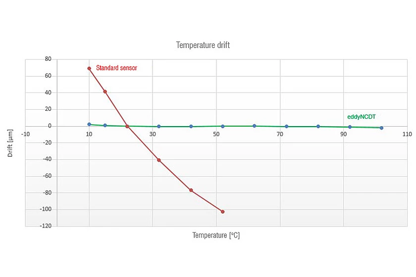
Best temperature compensation worldwide
The eddyNCDT 3020 compensates for temperature fluctuations in the vicinity of the controller between +10 and +105 °C which minimizes the influence on the measurement result. Temperatures on and around the sensor are even compensated up to +180 °C. This provides extremely high precision down to the nanometer range with excellent signal stability.
|
|
|
Configurable & easy to integrate
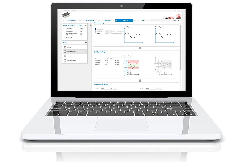
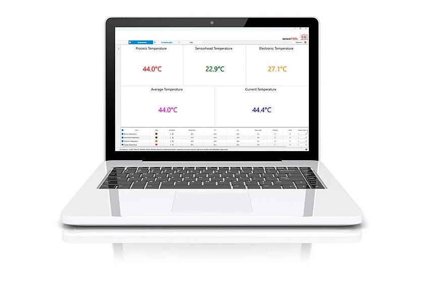
The eddyNCDT 3020 can be integrated via both digital and analog interfaces as well as via common fieldbuses. The free sensorTOOL is available for convenient configuration. Among other things, this software can be used to scale the analog output, store individual limit values for Condition Monitoring, activate averaging functions for signal smoothing or perform 3-point linearization to optimize measurement accuracy.
|
|
|
| |
 |
| |
|
|
| |
 |
|
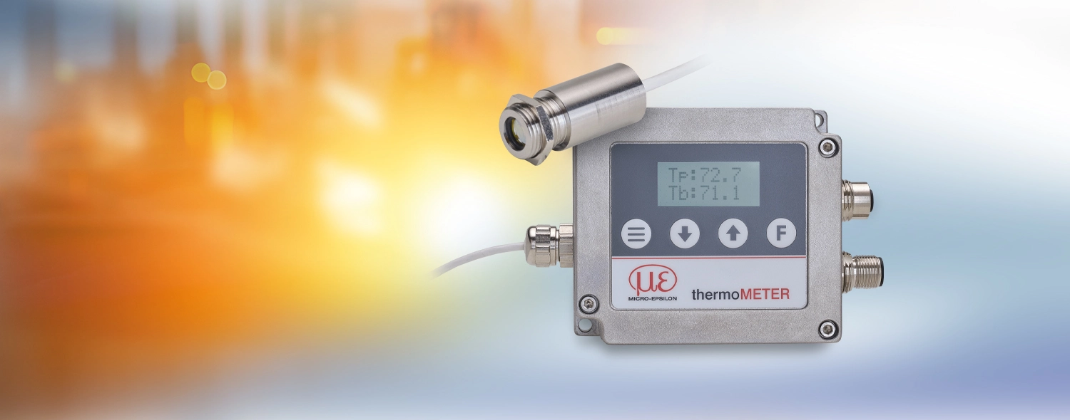
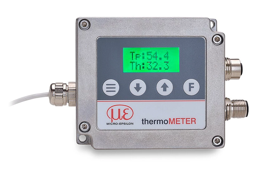
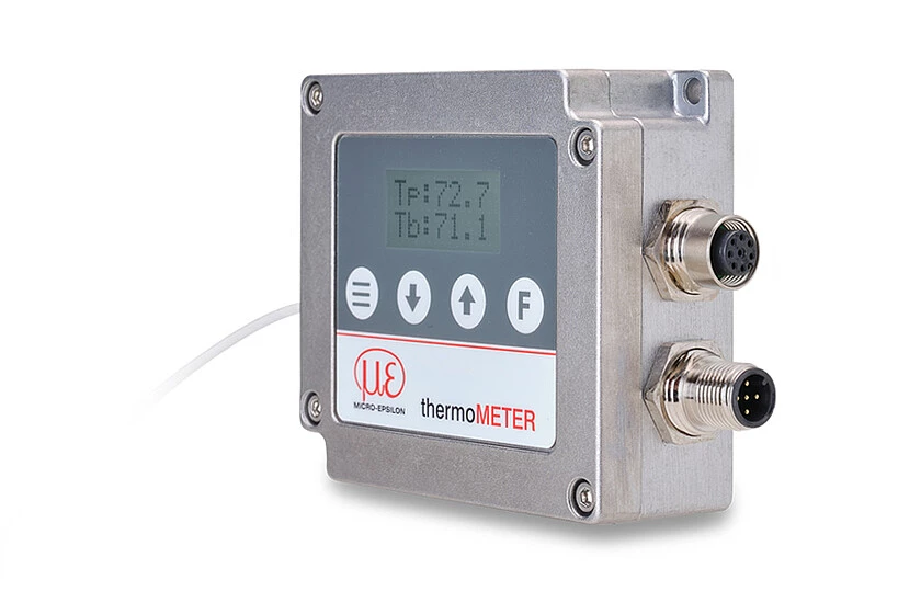
Fully integrated compact pyrometer for precise infrared temperature measurement
|
| |
|
Infrared pyrometers from the thermoMETER FI series are robust sensors for non-contact temperature measurement from -40 to +1100 °C. The combination of sensor & controller in one housing is extremely space-saving and simplifies integration. Its ease of use, extended configuration options via the sensorTOOL software and excellent price-performance ratio make the thermoMETER FI the ideal temperature sensor for OEM and series applications.
|
| |
|
|
| |
|
|
|
Fully integrated with extensive functions
The thermoMETER FI industrial pyrometers combine sensor and controller in a robust stainless steel housing, making them extremely compact. The integrated controller is extremely powerful and offers numerous setting options, which can be made via an optional USB converter and the sensorTOOL.
|
|
| |
The thermoMETER FI temperature sensors are extremely robust and can be used in environments up to +80 °C (even higher with cooling). Thanks to excellent temperature compensation, the industrial pyrometers measure extremely precisely, even at highly fluctuating ambient temperatures. In addition, high EMC immunity ensures that the measurement signal is not affected and remains stable even in industrial applications.
|
|
|
|
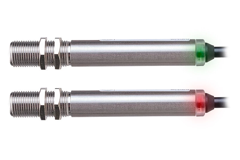
Quick setup and user-friendly operation
These precise temperature sensors are calibrated at the factory and preconfigured for a temperature range from 0 to +600 °C. Alarms or the system status can be recognized remotely via two integrated LEDs (red & green). An additional aiming aid function facilitates commissioning and helps to optimally align the sensor.
|
|
| |
| |
|
|
|
|
|
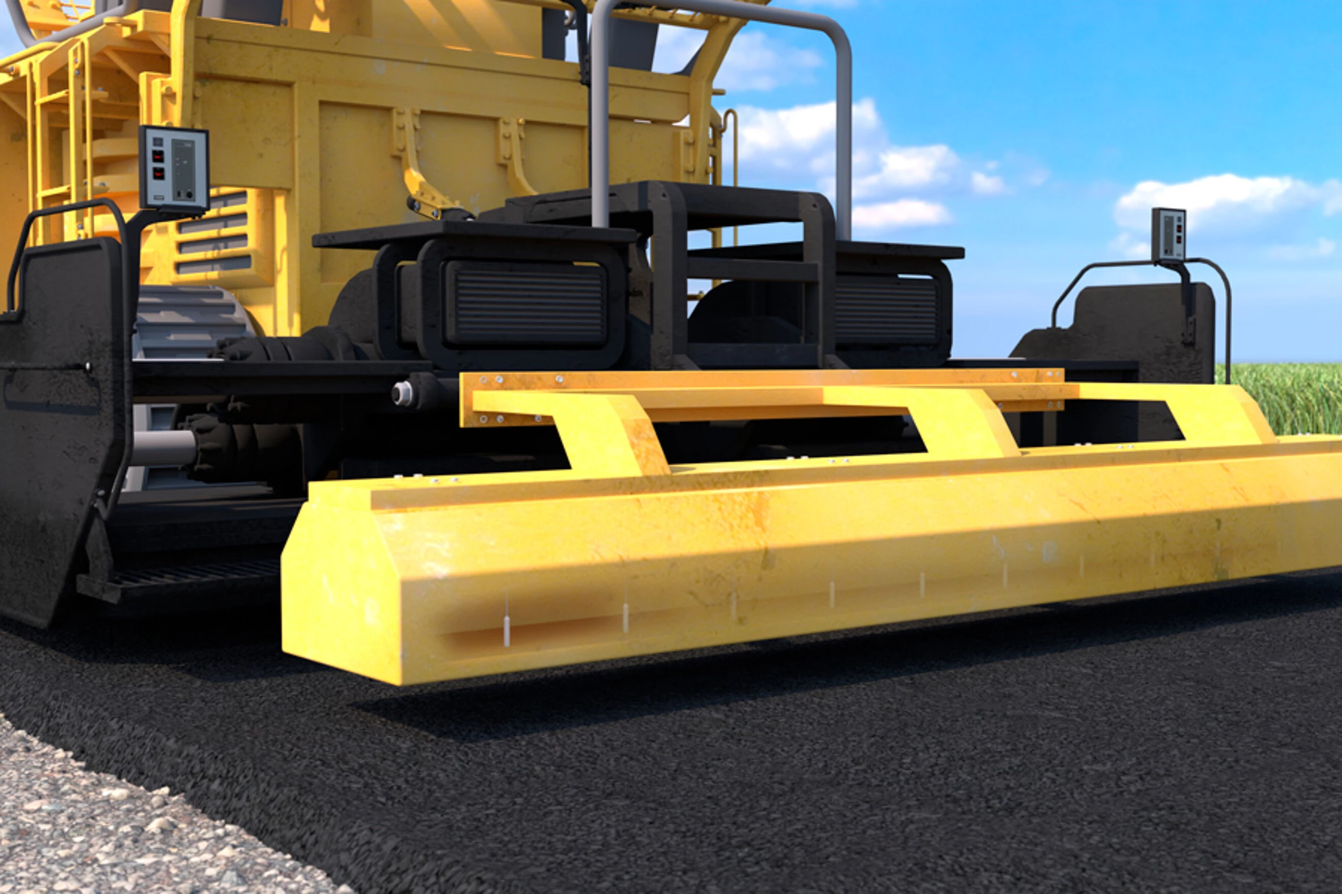
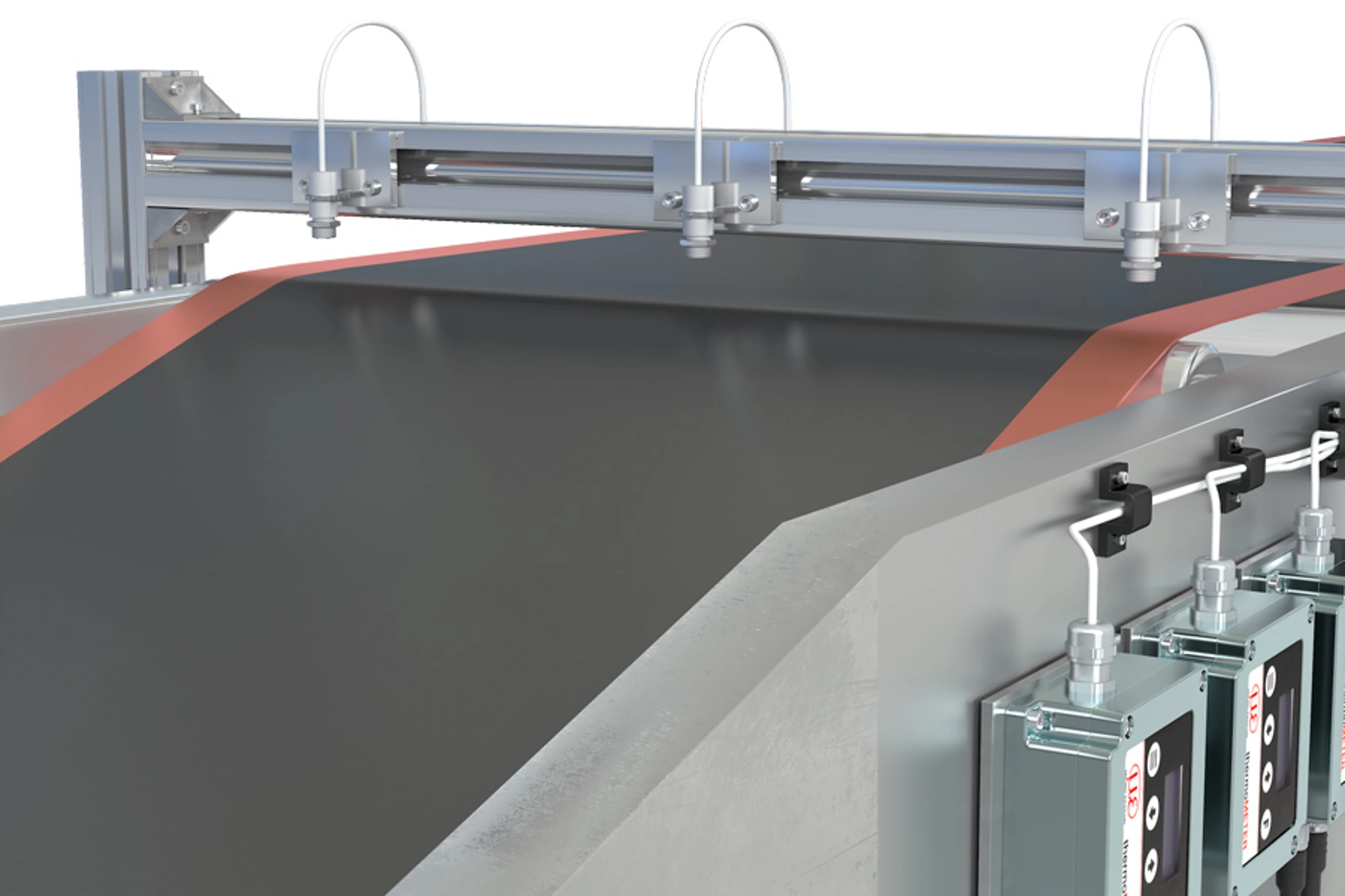
Integrated into asphalt pavers, thermoMETER FI pyrometers measure the asphalt temperature after application
|
|
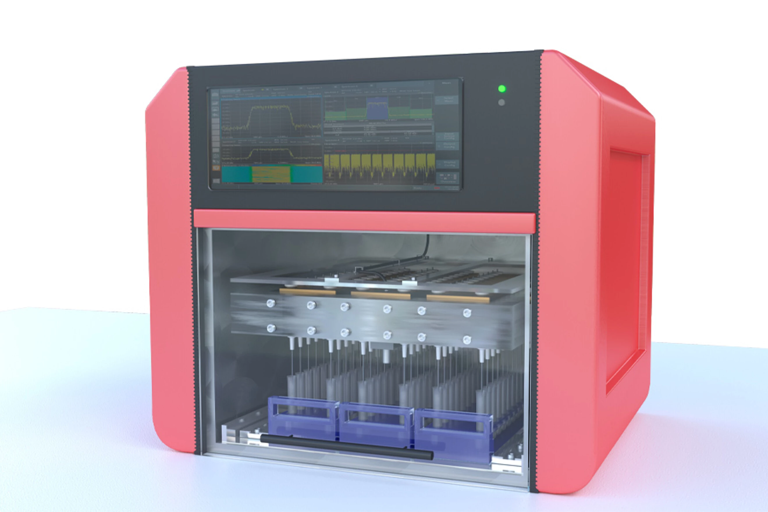
Measuring the temperature of samples in DNA analyzers with thermoMETER FI
|
|
| |
| |
|
 |
| |
|
|
| |
 |
|
Robust miniature pyrometers for non-contact infrared temperature measurements
|
| |
|
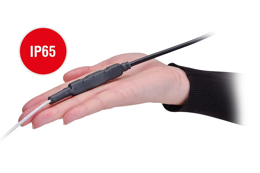
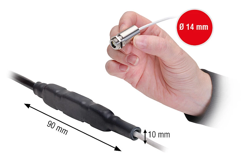
The thermoMETER SE is a precise infrared pyrometer for temperatures from -40 to +1100 °C. It consists of a compact sensor with a miniature controller integrated into the connection cable. The sensor itself is extremely small and can be used in hot environments up to 120 °C. In addition to its miniature design, robust construction and high performance, the thermoMETER SE is characterized by a wide range of interfaces and setting options. It is extremely versatile and is used in machine building and machine design, in production and for quality assurance. Due to its excellent price-performance ratio, it is particularly suitable for series applications and OEMs.
|
| |
|
|
| |
|
|
|
Lots of power - little effort
The thermoMETER SE industrial pyrometer is a complete and preconfigured measuring channel. The sensor, controller and connection cable are one unit that is calibrated and preconfigured at the factory, and therefore ready for immediate use. If required, the sensor can be parameterized via the sensorTOOL, which provides advanced settings and functions.
|
|
| |
The thermoMETER SE temperature sensors are extremely robust. As the controller is integrated in the cable, the sensor can be used in environments up to +120 °C (even higher with cooling). Thanks to excellent temperature compensation, the industrial pyrometers measure extremely precisely, even at highly fluctuating ambient temperatures. In addition, high EMC immunity ensures that the measurement signal is not affected and remains stable.
|
|
|
|
Compact sensor with miniature controller
Compact sensor with miniature controller
|
|
| |
| |
|
|
|

|
|
|
|
|
|
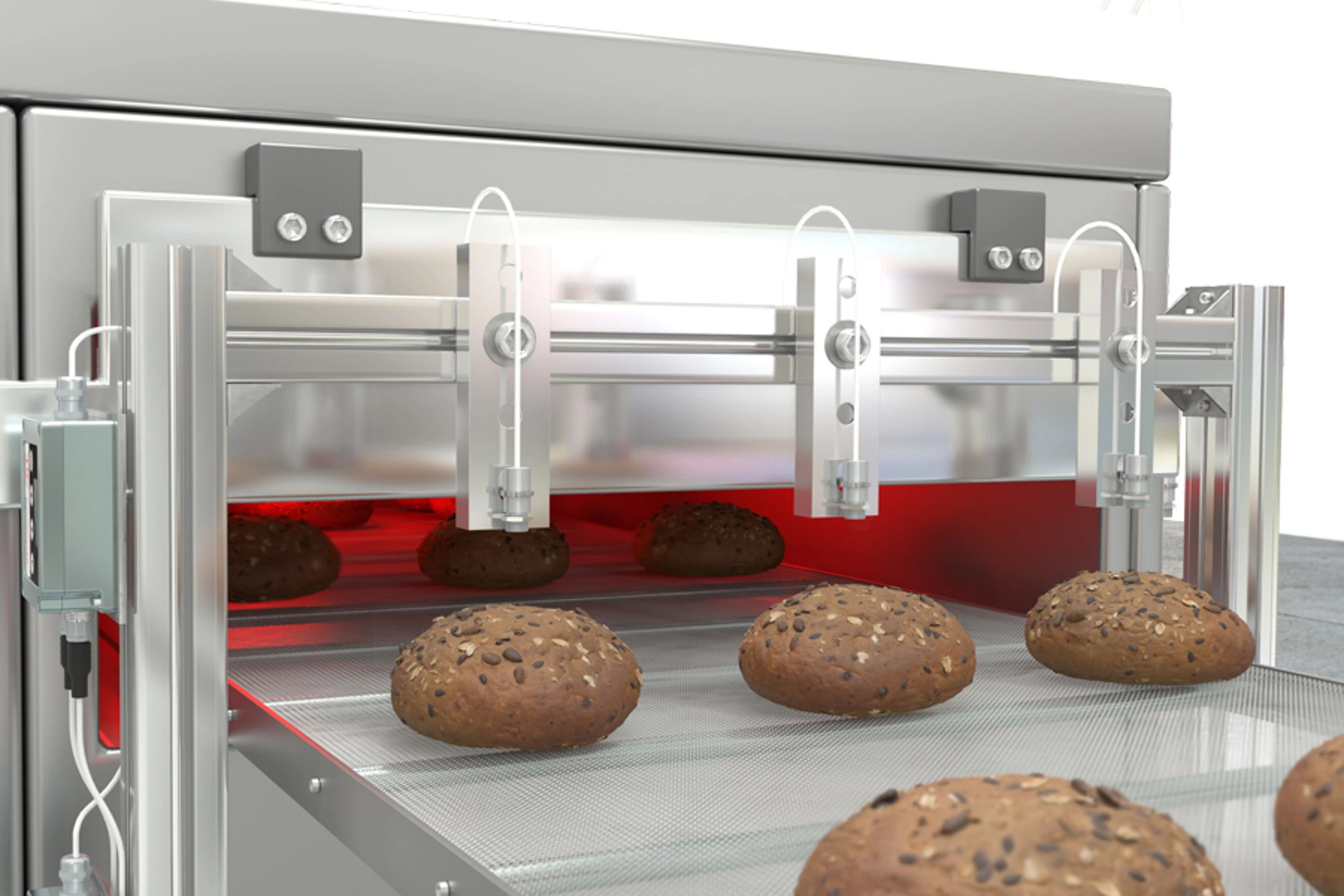
Measuring the temperature of baked goods with thermoMETER SE sensors
|
|
Checking the drying process after painting vehicles with thermoMETER SE
|
|
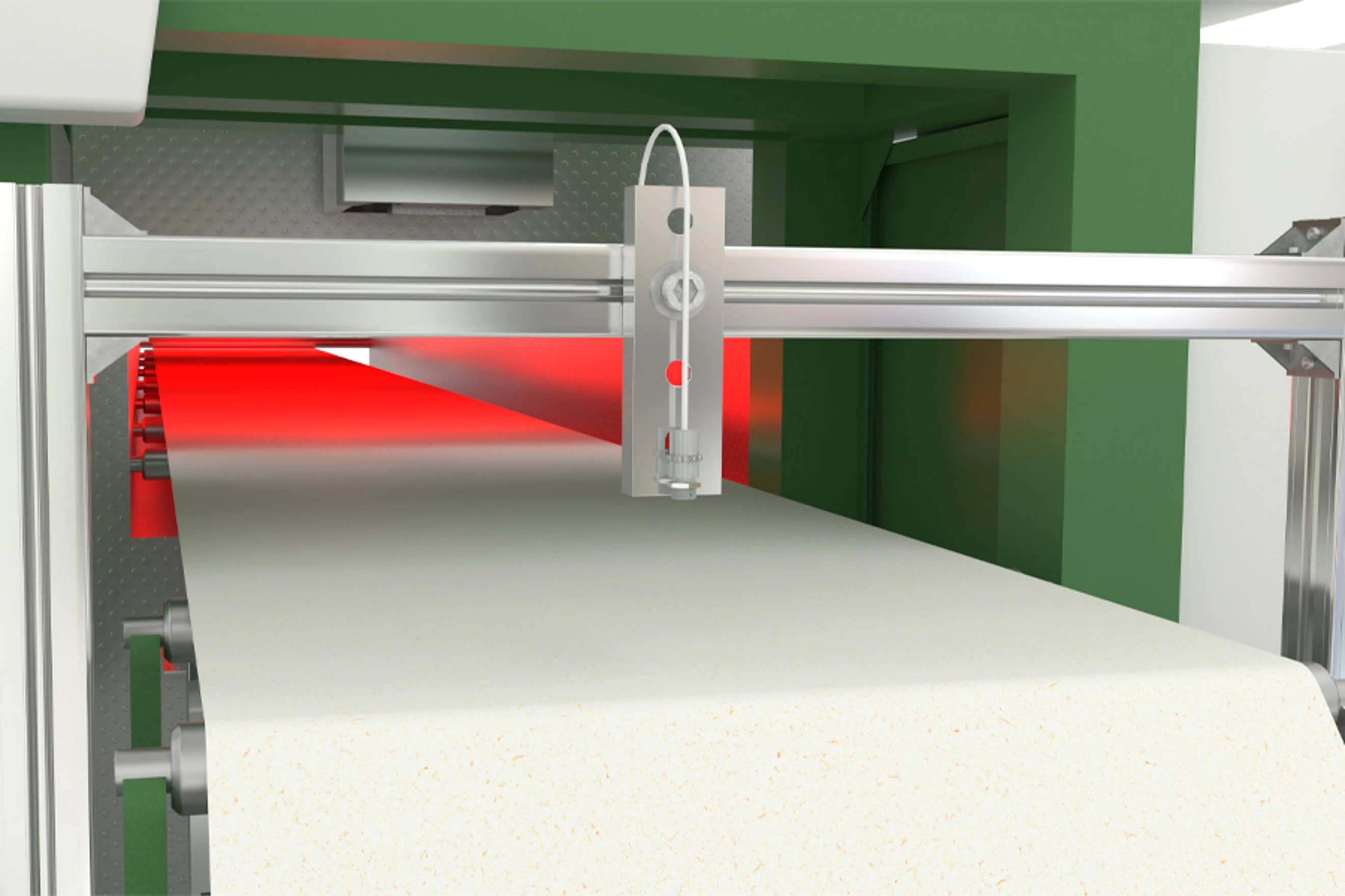
Monitoring the drying process in paper production with thermoMETER SE
|
|
Temperature measurement in the coating process of battery films with thermoMETER SE
|
|
| |
| |
|
 |
| |
|
|
| |
 |
|
High-performance industrial pyrometer for non-contact infrared temperature measurement
|
| |
|
The thermoMETER UC is an extremely powerful system for non-contact temperature measurement from -50 to +1.000 °C. It offers extensive functions and a modern design with standard M12 connections. The sensor is extremely small and can be used in environments with high temperatures up to 180 °C. Due to its high performance and robustness, it is primarily used in machine building and machine design, in production processes and for quality assurance. Various interfaces such as analog and digital outputs or switching and alarm signals offer numerous possibilities for integration into processes, machines and systems.
|
| |
|
|
| |
|
|
|
Flexible setup via display & keys or software
The robust controller in a die-cast aluminum housing has an integrated display with RGB backlight. The system can be set conveniently and easily using the large membrane keypad. Set alarm signals can be displayed via the backlight. As an option, sensorTOOL software is available free of charge for parameterization via a PC.
|
|
| |
Minimal installation effort
The controller of the thermoMETER UC has two M12 connections, which enable quick and easy wiring with standard industrial cables without having to remove the cover. The sensor is already permanently connected to the controller, whereby different cable lengths are available. The completeness of the cabling can be conveniently checked using a simulation mode. When mounting the sensor, an integrated aiming aid function supports the alignment of the sensor to the measuring object.
|
|
|
|
| |
|
|
|
Powerful pyrometer with extensive functions
The thermoMETER UC offers many functions and parameterization options for data acquisition, processing and output. For example, the emissivity of the measuring object can be calculated automatically for correct measurement recording. Intelligent averaging and filter functions are available for signal processing, as well as a calibration option via offset/gain. The output configuration is highly flexible. The desired alarm or analog output can be selected and scaled as required. Settings can be made for all processing stages of the temperature signal.
|
|
| |
| |
|