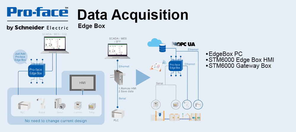
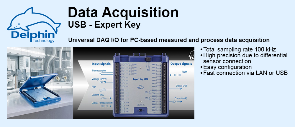
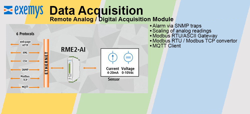
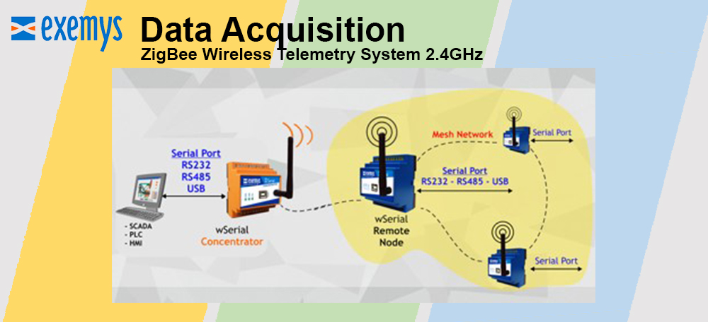
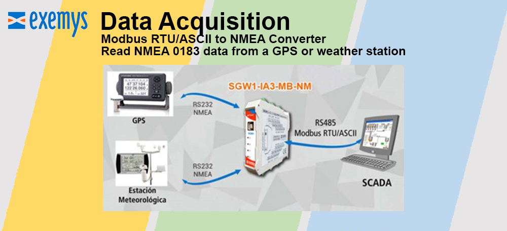
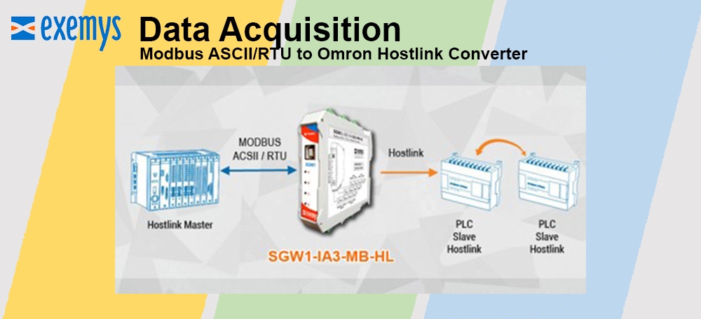
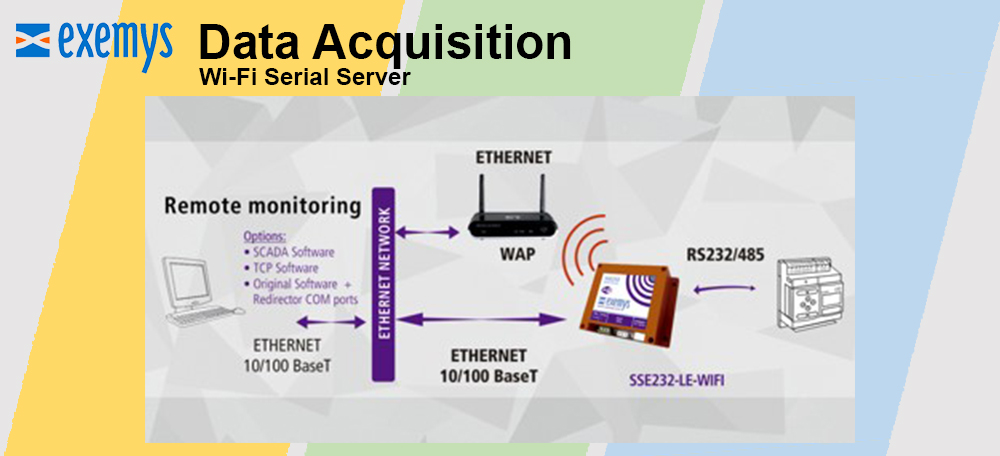
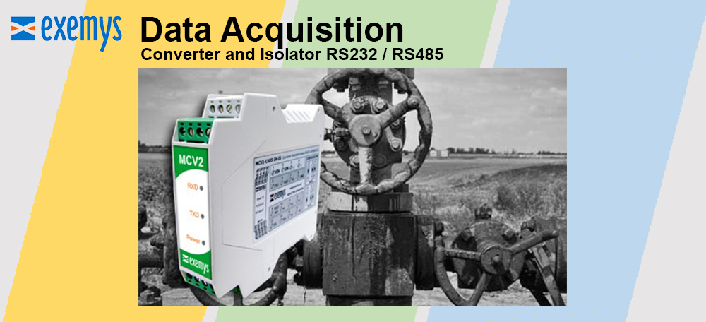
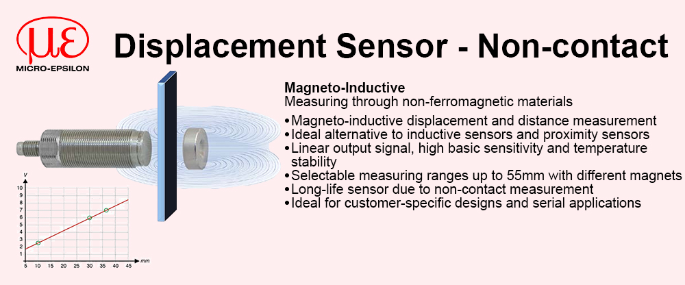
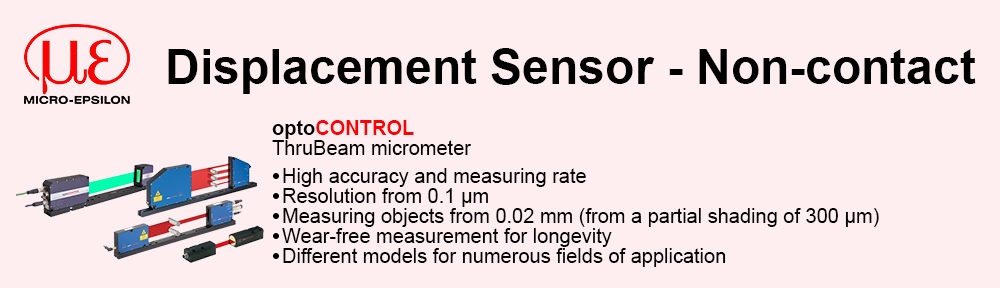
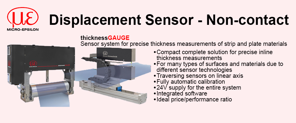
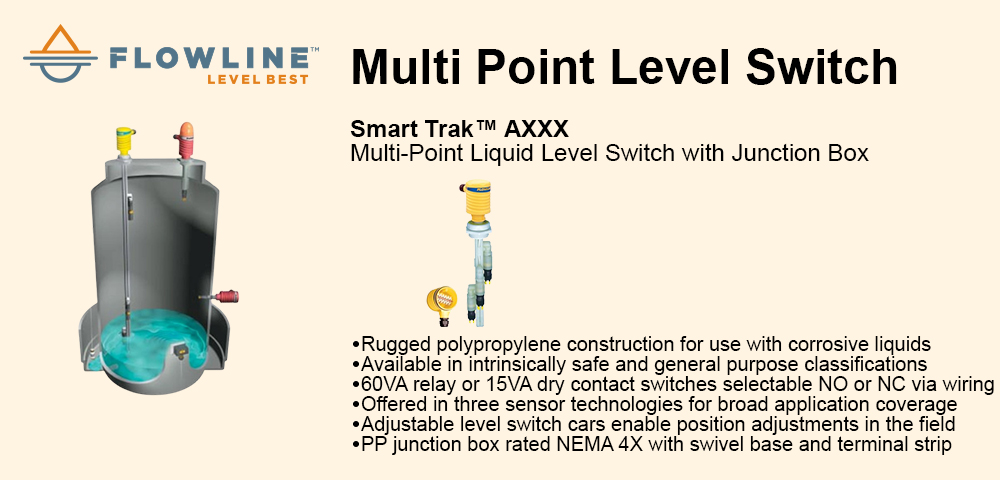
 |
|
|
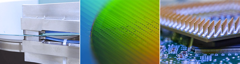
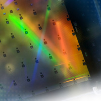
Semiconductors
|
|
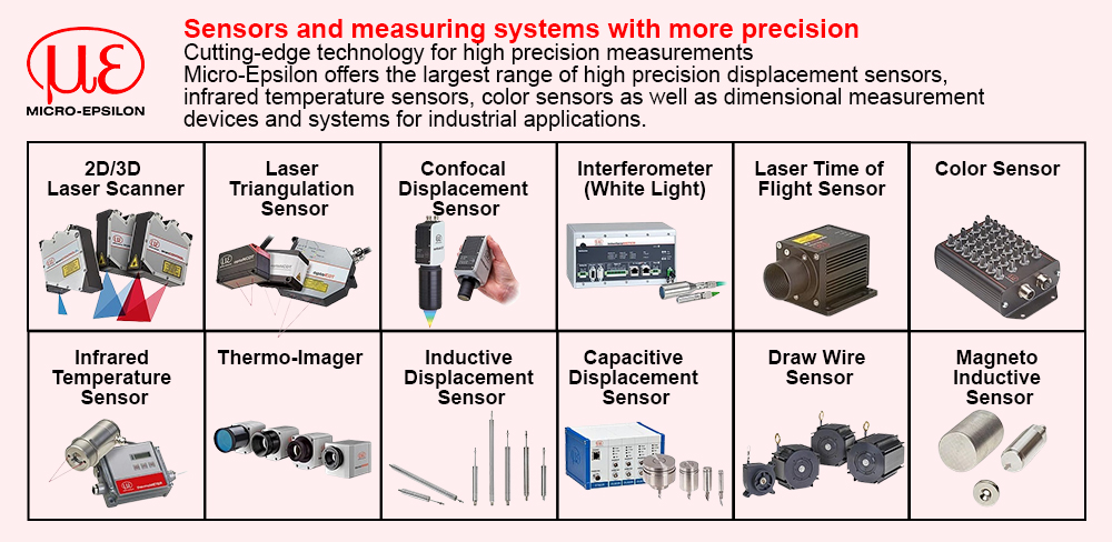
Measurement tasks in the semiconductor industry require highest accuracy and repeatability. Micro-Epsilon offers the right solution for numerous applications from precise machine positioning and wafer inspection to topographic measurements. |
|
|
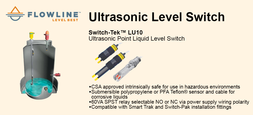
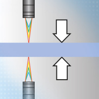
High precision thickness measurement of silicon wafers
|
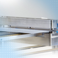 |
Capacitive displacement sensors are used for the exact thickness measurement of wafers. Two opposing sensors detect the thickness and also determine other parameters such as deflection or sawing marks. The position of the wafer in the measuring gap may vary.
 Capacitive displacement sensors and measurement systems Capacitive displacement sensors and measurement systems
|
|
|
|
Bow and warp of wafers
|
|
|
|
|
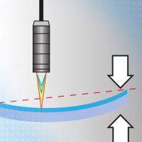
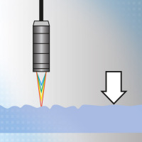
Detection and measurement of saw marks
|
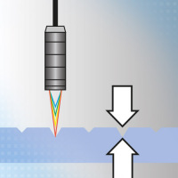 |
For automatic detection and measurement of saw marks, confocal chromatic sensors from Micro-Epsilon are used. The fast surface compensation feature of the controller regulates the exposure cycles in order to achieve maximum signal stability on surfaces with varying reflection characteristics. As confocal sensors from Micro-Epsilon can tolerate a large tilt angle and offer an extremely small light spot, they reliably detect saw marks and other indentations on the wafer.
Confocal sensor systems for displacement, distance, position and thickness
|
|
|
|
Recognition and measurement of bumps on silicon wafers
|
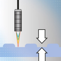 |
Confocal chromatic displacement sensors from Micro-Epsilon are used to inspect bumps. They generate a small light spot onto the wafer, while reliably detecting the smallest of parts and structures at high resolutions. Therefore, shape and dimensions of bumps are reliably measured for contacting purposes.
Confocal sensor systems for displacement, distance, position and thickness
|
|
|
|
Transparent layers & adhesive beading
|
 |
Confocal chromatic sensors are used for one-sided layer thickness measurements. The confocal measuring principle enables the evaluation of several signal peaks, allowing the thickness of transparent materials to be determined. With the multi-peak measurement feature, the confocalDT controller reliably determines the thickness of protective coatings and paint layers.
Confocal sensor systems for displacement, distance, position and thickness
|
|
|
|
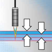
Wafer thickness measurement / TTV
|
 |
Confocal chromatic sensors measure the thickness deviation (Total Thickness Variation) and the wafer thickness from both sides. Based on the wafer thickness profile, bow and warp of the wafer can be detected. High measuring rates enable thickness detection of the entire wafer in short cycle times.
Confocal sensor systems for displacement, distance, position and thickness
|
|
|
|
Inspection of cracks and breakages
|
 |
Confocal chromatic sensors from Micro-Epsilon are used to detect cracks and other defects on the wafer. They reliably detect surfaces with varying reflection characteristics due to a fast surface compensation feature. An extremely small light spot and high resolution enable the reliable detection of the finest of anomalies on the wafer.
Confocal sensor systems for displacement, distance, position and thickness
|
|
|
|
Positioning of the lens system in lithography machines
|
 |
Non-contact, inductive displacement sensors (eddy current) measure the position of lens elements in order to achieve the highest possible imaging accuracy. Depending on the lens system, displacement sensors from Micro-Epsilon are used to detect movement and position in up to 6 degrees of freedom. Providing a high frequency response, eddyNCDT sensors also monitor highly dynamic movements of the lens system.
Inductive sensors (eddy current) for displacement, distance & position
|
|
|
|
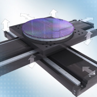
Positioning the wafer stage
|
|
|
|
|
Nanometer positioning in lithography machines
|
 |
To illuminate individual components on the wafer, the lithographic devices move the wafer to the respective position. Capacitive displacement sensors measure the position of the travel path in order to enable nanometer-accurate positioning.
Capacitive displacement sensors and measurement systems
|
|
|
|
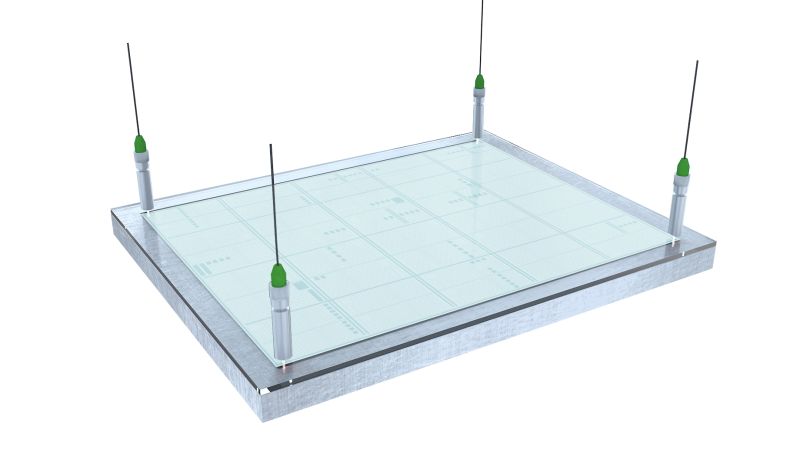
Positioning of masks in lithography
|
 |
Lithography processes require high resolution and long-term measurement of machine movements in order to achieve maximum precision. High resolutions enable nanometer-precise positioning of masks using capacitive sensors from Micro-Epsilon. Their vacuum-suitable design enables the sensors and cables to be used in ultra-high vacuum.
capaNCDT 6200
|
|
|
|
|
|